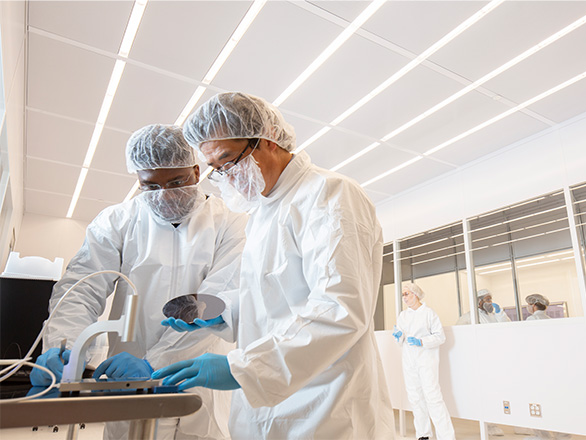
Davidson Foundation Cleanroom
What is it?
The College of Engineering’s Class 1,000 Cleanroom provides 2,937 square feet of filtered space available for faculty and industry research. This multi-user facility offers lithography, deposition, etch and metrology to support research and pilot production of semiconductor, photonic and quantum devices. Our Bio Bay is also specially configured to support biological research.
Equipment
The Cleanroom is outfitted with various machinery to suit the needs of a variety of users. Learn more about our equipment:
The Essemtec Fox is a compact and versatile pick-and-place system designed for high-mix surface mount technology (SMT) assembly. It eliminates the need for a solder paste screen printer by jet dispensing solder paste before placing SMT components. The feeder system can be configured for up to 200 lanes and accepts tape, stick, strip, and tray sliders for components ranging in size from 01005 to 80 mm x 80 mm x 25 mm. The ePlace software converts design files for production and enables all-in-one job planning, setup optimization, stock management, data analysis, line management, and component traceability. Additionally, the Fox can be reconfigured with a time pressure, screw rotation, volume dispenser, or piezo jet valve for a variety of dispensing applications like underfill, glob top, encapsulation, gasketing, dam and fill, and adhesives. When combined with a DragonFly IV and a multizone reflow oven like the Essemtec Lizard, a variety of fully functional PCB designs can be fabricated and assembled in-house with minimal changeover times.
The Oxford Instruments Cobra is perhaps the highest performance R&D etch system in the academic world. Our system is configured with two atomic layer etch manifolds, cryogenic capability and optical emission spectroscopy (OES). We are the first research facility in the world to have an etch system with all of these capabilities. The system allows our users to etch nearly any material imaginable quickly (ICP RIE mode), with atomic layer precision (ALE mode) and with ultra-low roughness high aspect ratio sidewalls (cryogenic mode). This system has both chlorine and fluorine chemistries and will support both standard user applications and a research program in cutting-edge next generation atomic layer etch processing.
Our electron beam evaporator enables deposition and patterning of metals without the need for etch processes. The long metal-substrate distance ensures that evaporated material strikes the substrate at a nearly 90-degree angle, which allows the use of shadow masks and specialized negative-profile photoresists for liftoff processing. For many users, this tool is the easiest path to a functioning device. Our system can deposit up to six materials without breaking vacuum and has in-situ thickness measurement capability. It is also configured with a cryogenic pumping system for a lower base pressure.
Sputtering is a deposition process in which a plasma is used to ablate material from a metal or dielectric target. The ablated material redeposits onto the substrate. Sputtering is a more flexible technique than evaporation and enables deposition of insulating materials such as oxides and nitrides, in addition to metals. The tradeoff is that sputtered films are rarely compatible with liftoff processes and thus must be etched, and in-situ thickness measurement is not straightforward. Our system is configured with three 3-inch targets, a loadlock, RF power for deposition of oxides and in-situ etch/clean, and pulsed DC power for deposition of nitrides and metals.
The Nano Dimension DragonFly IV is an industrial system for producing additively manufactured electronics (AME), which includes traditional multi-layer printed circuit boards (PCBs) and 3D electronic designs. It uses hundreds of piezo inkjet nozzles to deposit both silver nanoparticle conductive ink (CI) and photopolymer dielectric ink (DI). The CI is infrared sintered, and the DI is UV cured. The minimum recommended layer thickness of 10 um combined with an 18 µm x 18 µm print resolution enables a minimum XY feature size of 36 µm x 36 µm, minimum trace width of 75 µm and spacing of 100 µm. The conductive material has an electrical conductivity similar to copper, and the dielectric material has a uniform dielectric constant and loss tangent up to 65 GHz, enabling a variety of applications from DC to RF. The DragonFly IV enables in-house prototyping of devices up to 160 mm x 160 mm x 3 mm with shorter lead time than a traditional PCB manufacturing process which involves drilling, etching, and electroplating. It also provides users the flexibility to design 3D features that are not typically possible. The system is compatible with mechanical and electrical CAD software, taking ODB++, Gerber, Excellon, and STL files as inputs.
In-line metrology is distinguished by its ease of use and non-destructive nature. These are the measurements we take between process steps. Our facility offers four-point probe for sheet resistance measurement, refractometry for photoresist thickness measurement, non-contact profilometry, optical microscopy and more as part of our growing metrology suite. We also can assist our users in gaining access to complementary University of Nevada, Reno equipment such as SEM/EDS, FIB, AFM, nanoindentation, XPS and XRD.
Usage policies
Pricing and membership policies will be posted in late 2024, and will evolve based on equipment availability and user needs. Please contact the facility director if you are interested in using the facility.
Contact
Russ Renzas, Cleanroom Director
College of Engineering
rrenzas@unr.edu
Russ Renzas is an expert in materials science, atomic layer processing and superconducting quantum circuit fabrication. He has coauthored over 20 academic papers with over 3,500 citations and two patents. Renzas was previously director of Device Fabrication at Rigetti Computing, a venture-backed superconducting quantum computer manufacturer now listed on NASDAQ. He has given invited seminars at leading national labs and universities worldwide, including Harvard, Yale, Caltech, Fermilab, PSI and IIT Delhi. He has a BSE in electrical engineering from Princeton University (2005) and a Ph.D. in physical chemistry from the University of California, Berkeley (2010). Renzas has lived in Reno since 2020. Outside the lab he enjoys Nordic skiing, snowboarding, whitewater kayaking, complex board games, volunteering in the community and occasionally assisting with technical due diligence for angel investment opportunities with Princeton Alumni Angels.