Researchers will be able to push the boundaries of semiconductors, photonics and other nanofabricated technology when the Davidson Foundation Cleanroom opens later this year in the William Pennington Engineering Building.
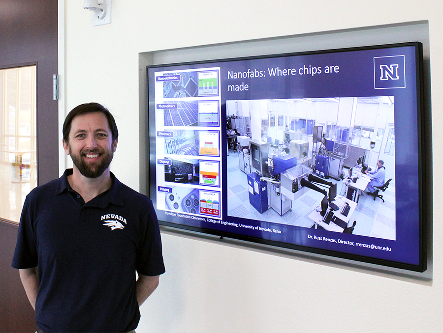
Russell Renzas, the Cleanroom’s new director, holds a doctorate in physical chemistry from the University of California, Berkeley, and has over a decade of industry experience. Since joining the University of Nevada, Reno in January, he has been equipping the facility with tools and equipment necessary for nanofabrication. Nanofabrication is the manufacture of materials with nanometer dimensions — basically, items that are one-millionth of a meter. Nanofabrication processes are used in the manufacturing of modern integrated circuits of all kinds, ranging from silicon-based transistor technology to quantum devices.
The Davidson Foundation Cleanroom will be the only one of its kind in the northern Nevada region, and is expected to support current and future local industry by offering access to cutting-edge research and prototype capabilities and developing a workforce trained in critical nanofabrication skills.
“This facility is going to change the trajectory of technology innovation here in northern Nevada,” Renzas said. “We will perform cutting-edge research, train a future workforce, inspire and spin off new companies and accelerate our region’s growth as a technology hub.”
The Cleanroom and its operations support the College of Engineering’s research pillar addressing resilient supply chains and critical materials, including semiconductors and batteries.
“We are excited to see movement in this project,” Engineering Dean Erick Jones said. “When the Davidson Foundation Cleanroom is operational, it will dramatically expand our research capabilities, enrich the academic opportunities for our students and transform the region’s tech industry.”
Starting small
Nanofabrication deals with the properties of atoms in a material. The process typically begins with a silicon wafer about a few inches in diameter, upon which are deposited tens or hundreds of nanometers of metal or dielectric material (material that is a poor conductor of electricity but an efficient supporter of electrostatic fields).
The wafer is then coated with a light-sensitive polymer called photoresist, Renzas explained. After that, some portions of the photoresist are exposed to light through a mask. Those exposed portions are chemically weakened, allowing them to be easily removed, thus revealing selected portions of the deposited material below.
The exposed material is etched with a plasma etching system, and the process is finished by removing the remaining photoresist.
“Repeated cycles of this process, with some variations, allow us to manufacture complex miniature electronic, photonic and quantum circuits,” Renzas said.
The result can be faster, smaller and more powerful computers and electronics. Among the Engineering research faculty working in this area are Jeongwon Park and Hao Xu, both associate professors in Electrical & Biomedical Engineering; Maryam Raeeszadeh-Sarmazdeh, an assistant professor in Chemical & Materials Engineering; and Renzas himself, who is adjunct faculty in Chemical & Materials Engineering and conducts research in atomic layer etch and superconducting quantum circuits.
Renzas also sees the new Cleanroom as a complimentary facility to some of the University’s existing research labs and equipment, such as the Electronic Microscopy and Microanalysis Facility in the College of Engineering’s department of Chemical & Materials Engineering.
How clean is a cleanroom?
Because nanofabrication happens at the atomic level, the process must be conducted in dust-free environments.
Most of the Davidson Foundation Cleanroom’s 2,937 square feet is rated Class 1000, which means there are less than 1,000 particles per cubic meter of air. The lithography bay, where some types of masking and etching are conducted, is Class 100.
“This level of cleanliness requires, essentially, a gigantic HVAC system to push air through HEPA (high efficiency particulate air) filters into the cleanroom,” Renzas said. “And then pull it out through the service chases, as well as to control the temperature and humidity of the air.”
Looking ahead
As Renzas works to equip the cleanroom with the necessary equipment, he is also working to develop partnerships with industry and research institutions that will make the facility a robust center for innovation. Cleanroom machinery currently on order includes:
- an ICP RIE etch system from Oxford Instruments uniquely configured with two atomic layer etch manifolds, cryogenic capability and optical emission spectroscopy.
- A maskless lithography system which enables photoresist patterning without the need for costly physical masks.
- An electron beam evaporator that enables deposition and patterning of metals without the need for etch processes.
- A sputtering system used in a deposition process in which a plasma is used to ablate material from a metal or dielectric target.
- A 3D circuit printer which can create flex and standard PCB boards with buried features not possible using standard PCB fabrication techniques.
“It’s going to take time,” Renzas said. “This is going to be a great journey, and we’ll be growing fast.”
For more information, reach out to Russell Renzas at rrenzas@unr.edu.


